The 12th edition of Graphene Conference series, the largest European Event in Graphene and 2D Materials, will be organized in-person in Aachen, Germany on July 5-8, 2022. Over the past editions, the Graphene Conference strengthened its position as the main in-person meeting point of the Graphene community Worldwide. Step by Park Systems booth to talk about advances in investigating 2D materials in nanorange!

Join Alexander Klasen, Principal Scientist from Park Systems Europe at Graphene 2022 for his talk:
- ⏩ TALK: “Exploring the Interplay of Layered Materials: Atomic Force Microscopy as a Path to Morphology and Functional Properties of Heterostructures”
- ⏩ DATE: Wednesday, 6 July, 11am, Session: Industrial Forum
- ⏩ BOOTH No.: 20
ABSTRACT
Exploring the Interplay of Layered Materials: Atomic Force Microscopy as a Path to Morphology and Functional Properties of Heterostructures
Presenting Author: Alexander Klasen1
Co-Authors: James Kerfoot1, Andrea Cerreta1
1Park Systems Europe GmbH, Mannheim, Germany

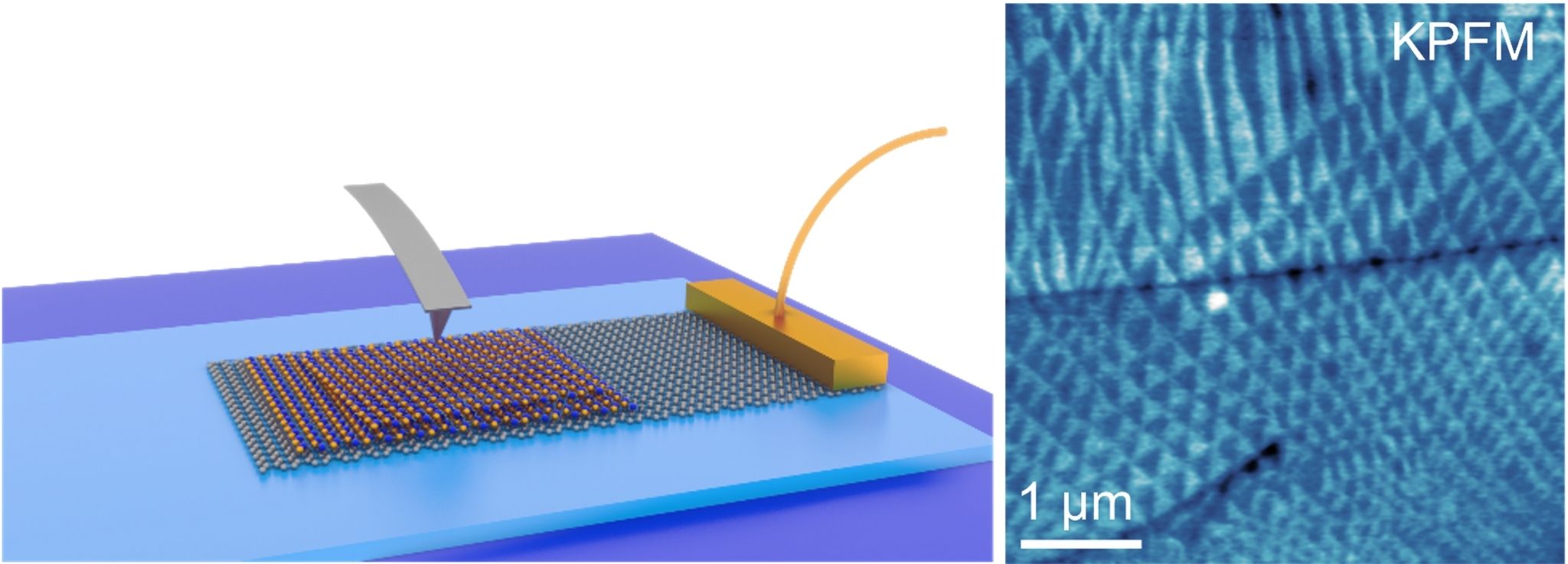
Figure 1: Example of the electrostatic characterization of layered heterostructures using AFM: Mapping of interfacial ferroelectricity in parallel stacked hBN using KPFM.
Heterostructures of 2D materials often are more than the mere sum of their parts. Novel mechanical, electronic and optical properties can arise from the interplay of stacked 2D structures. This becomes particularly evident when orientation mismatch or strain between subsequent layers significantly modifies the properties of the involved materials with respect to bulk. Such complex phenomena require equally versatile means of characterization that allow studying such features on a local scale, be it functional parameters like the morphology, conductance, surface potential, piezoelectricity, or local mechanic features like stiffness and adhesion. Atomic force microscopy (AFM) has been established as a most versatile tool since it allows to quantitatively measure a holistic pool of parameters non-destructively with sub-nanometer resolution. In this talk, we provide several state-of-the-art examples for the fundamental characterization of layered 2D heterostructures using AFM. As introduced in several recent accounts, stacks of graphene and hexagonal boron nitride (hBN) can be deposited on Si/SiO₂ with a controlled twist angle to give rise to different properties ranging from moiré pattern in the local conductance [1,2] to ferroelectric superlattices [3-5]. We describe the characterization of ferroelectric domains in such parallel stacked hBN by both electrostatic force microscopy (EFM) and Kelvin probe force microscopy (KPFM) in addition to manipulation of these domains by applying a bias to the sample via the AFM probe. These highly resolved electrical measurements can be further correlated with local mapping of the nanomechanical response of the sample, providing a complete set of information about the properties of hBN and similar 2D materials and allowing their optimization for applied research.
References
[1] C. R. Woods et al., Nature Phys, 10 (2014) 451-456
[2] R. Ribeiro-Palau et al., Science, 361, 6403 (2018) 690-693
[3] C. R. Woods et al., Nat Commun., 12 (2021) 347
[4] K. Yasuda et al., Science, 372, 6549 (2021) 1458-1462
[5] M. Vizner Stern et al., Science 372, 6549 (2021) 1462-1466
