-
Annealing Mapping Barium_titanate HighResolution GaN AIN Lift OxideLayer doped dielectric trench Battery Oxide Microchannel Pzt PolyvinylAcetate Transparent Sidewall hard_disk_media Polyimide PrCurve LateralForceMicroscopy MESA structure Fiber Crystal PFM #Materials UnivCollegeLondon Bacteria Dental PvdfFilm CntFilm ring shape Magnets ScratchMode Filter
Report image
If you found this image unacceptable, please let us know. We will review your report and take action if we determine this image is really unacceptable.
Multi-layer necking device defect
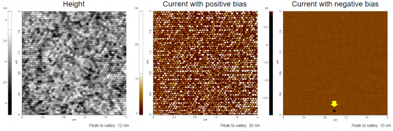
Scanning Conditions
- System : NX-Wafer
- Scan Mode: C-AFM
- Scan Rate : 2Hz
- Scan Size : 2μm×2μm
- Pixel Size : 512×256
- Cantilever : AD-2.8-AS (k=2.8N/m, f=75kHz)