-
Anneal Heat LMF TemperatureControl Piranha Liquid conductive Bio GlassTemperature PetruPoni_Institute optoelectronics PhaseTransition Potential AlkaneFilm F14H20 Tin disulfide CuSubstrate Thermal hard_disk_media Copolymer StyreneBeads Materials PrCurve Phosphide Chemical Vapor Deposition FrictionalForce self-assembly Gallium_Arsenide STO Sadowski Iron Metal-organicComplex self-assembled_monolayer Pinpoint PFM LateralForceMicroscopy
Report image
If you found this image unacceptable, please let us know. We will review your report and take action if we determine this image is really unacceptable.
hBN-few layer Graphene
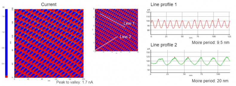
Scanning Conditions
- System : NX10
- Sample bias: 1.75 V
- Scan Mode: C-AFM
- Scan Rate : ALL 0.5Hz
- Scan Size : 200nm×200nm
- Pixel Size : 2048×2048
- Cantilever : AD-2.8-AS (k=2.8N/m, f=75kHz)