-
ShenYang MeltingPoint NiFe CVD BCZT molecule Ferroelectric Heating InLiquid IMT_Bucharest Tape Modulus Solar Hysteresys Platinum CeNSE_IISc LightEmiting vertical_PFM ConductiveAFM Chromium SmalScan TPU SmallScan Ananth FuelCell pinpoint mode CP-AFM ThermalProperties Fluoride Alloy Polyvinylidene GaN MfmPhase CrystalGrowing self_healing
Report image
If you found this image unacceptable, please let us know. We will review your report and take action if we determine this image is really unacceptable.
MoSi₂ Hard defect repair
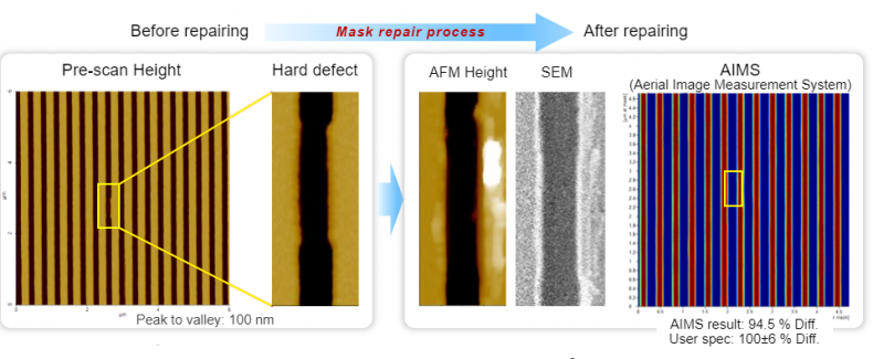
Scanning Conditions
- System : NX-Mask
- Scan Mode: Non-contact for imaging Sweep for repairing
- Scan Rate : 0.3 Hz
- Scan Size : 6μm, 0.5μm×1μm
- Pixel Size : 512×64 for 6μm2, 512×34 for 0.5μm×1μm