-
ElectroDeposition fluoroalkane CarbonNanotube Vortex HardDiskMedia Oxide Hexylthiophene optoelectronics SiliconCrystal Chemical_Vapor_Deposition P3HT Laser Optoelectonics LifeScience Platinum Nickel Vac Carbon NanoLithography GalliumPhosphide EvatecAG StainlessSteel organic_polymer Polydimethylsiloxane semifluorinated_alkanes ThermalProperties Melt Strontium CuParticle temp KevlarFiber OpticalElement molecules InLiquid SRAM
Report image
If you found this image unacceptable, please let us know. We will review your report and take action if we determine this image is really unacceptable.
Taegeuk Mark Lithography on PZT
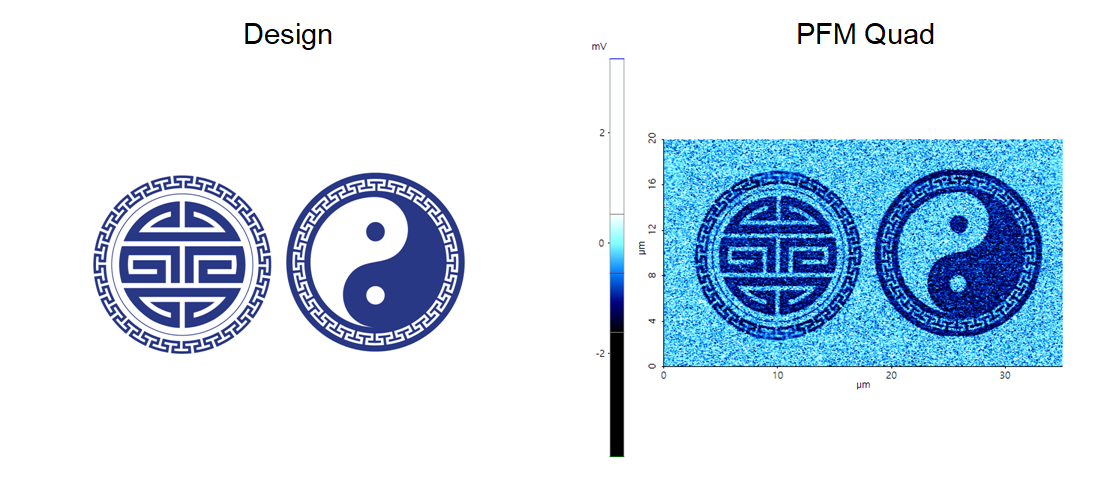
Re-arranged the domain pole direction on PZT surface using bias mode of lithography.
Scanning Conditions
- System: NX10
- Scan Mode: Lithography
- Cantilever: PPP-ContScPt (k=0.2N/m, f=25kHz)
- Scan Size: 35μm×20μm
- Scan Rate: 0.5Hz
- Pixel Size: 1024 × 1024
- Tip Bias: 10V for patterned area
- Scan Mode: Lithography
- Cantilever: PPP-ContScPt (k=0.2N/m, f=25kHz)
- Scan Size: 35μm×20μm
- Scan Rate: 0.5Hz
- Pixel Size: 1024 × 1024
- Tip Bias: 10V for patterned area